
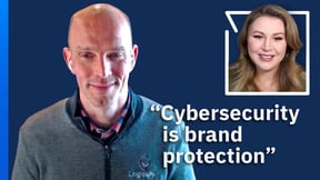
Logically CEO Joshua Skeens discusses board-level cyber risk, brand protection, tool sprawl, AI ROI, and MSP strategy.
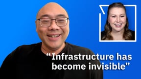
Katie Bavoso sits down with MK Tong, CEO of SotaTek USA, to break down why infrastructure—not AI models—is the real bottleneck for enterprise success
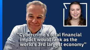
SecurityBridge CEO Jesper Zerlang discusses SAP security, AI risks like data poisoning, and why channel partnerships are key to 2026 growth.
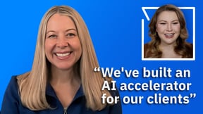
Spyglass MTG CEO Dori Albert explains how organizations can build secure and data-driven AI platforms that deliver real business value.
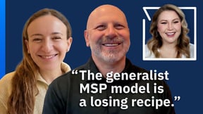
Leaders from Harbor IT explain why the traditional generalist MSP model is fading and how specialization, cybersecurity expertise, and vertical industry focus are shaping the future of managed services.
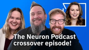
In this Channel Insider crossover, the hosts of The Neuron break down the AI race, the bubble debate, and what today’s tools really mean for businesses and everyday users.

-
Channel Business -
Security -
AI -
Infrastructure Related Topics -
- Lists & Awards Top ArticlesLink to AI 50 List AI 50 ListChannel Insider's editorial team spotlights the top AI leaders from MSPs, vendors, and channel businesses delivering measurable outcomes.Link to CML 100 Honorees
 CML 100 HonoreesCheck out our CML 100 List to discover the top channel marketing individuals who are transforming channel marketing for their organizations.Link to HSP 250 List HSP 250 ListView our HSP250 list to see the top Hybrid Solution Providers that have proactively embraced the future of tech.Link to The 2024 Channel Insider VIP List The 2024 Channel Insider VIP ListChannel Insider sought nominations from IT vendors, solution providers, and partners to highlight impactful collaborations. Check out our top choices here.
 - Resources Resource HubsFeatured ResourcesLink to Logically CEO on Cyber Risk, AI, and MSP StrategyLogically CEO on Cyber Risk, AI, and MSP Strategy
Logically CEO Joshua Skeens discusses board-level cyber risk, brand protection, tool sprawl, AI ROI, and MSP strategy.
Link to Video: SotaTek US CEO on AI Infrastructure Mistakes MSPs Must FixVideo: SotaTek US CEO on AI Infrastructure Mistakes MSPs Must FixKatie Bavoso sits down with MK Tong, CEO of SotaTek USA, to break down why infrastructure—not AI models—is the real bottleneck for enterprise success
Link to Video: SecurityBridge CEO on SAP Security, AI Risks & 2026 PrioritiesVideo: SecurityBridge CEO on SAP Security, AI Risks & 2026 PrioritiesSecurityBridge CEO Jesper Zerlang discusses SAP security, AI risks like data poisoning, and why channel partnerships are key to 2026 growth.
Link to Video: Why Most AI Projects Fail According to Spyglass MTG CEOVideo: Why Most AI Projects Fail According to Spyglass MTG CEOSpyglass MTG CEO Dori Albert explains how organizations can build secure and data-driven AI platforms that deliver real business value.
Link to Video: Harbor IT on NENS Acquisition and Why the Generalist MSP Model Is DyingVideo: Harbor IT on NENS Acquisition and Why the Generalist MSP Model Is DyingLeaders from Harbor IT explain why the traditional generalist MSP model is fading and how specialization, cybersecurity expertise, and vertical industry focus are shaping the future of managed services.
Link to Video: Hype, Bubble, or Breakthrough? Talking All Things AI with The NeuronVideo: Hype, Bubble, or Breakthrough? Talking All Things AI with The NeuronIn this Channel Insider crossover, the hosts of The Neuron break down the AI race, the bubble debate, and what today’s tools really mean for businesses and everyday users.
- About About
- Events Events